 Hardware Description Languages
# 本章内容
4.1 Introduction
4.2 Combinational Logic
4.3 Structural Modeling
4.4 Sequential Logic
4.5 More Combinational Logic
4.6 Finite State Machines
4.7 Data Types*
4.8 Parameterized Modules*
4.9 Testbenches
4.10 Summary
警告
在 system verilog 中有数据类型 logic,verilog 中没有数据类型 logic。本节使用了 system verilog 描述,把本节 system verilog 代码中的
logic类型符去掉就可以变为 verilog 语言描述。verilog 中没有
always_ff,always_latch,always_comb. 具体见 register
# 4.1 Introduction
HDL(Hardware Description Language)
HDL 语言用来描述电路的逻辑功能,然后 CAD (computer-aided design) 可以根据 HDL 语言的描述实现对应的逻辑门电路。
本章重点:

# 4.1.1 Modules
Modules (模块): 一块具有输入输出的硬件叫做 Modules。
两种描述模块的方法: behavioral & structural
behavioral: 描述一个模块的是用来干什么的,即描述模块的行为,输入输出的关系 (4.2 节进行介绍)
structural: 描述一个模块是如何组成的,即描述模块的结构,如果使用简单的模块构建复杂的模块 (4.3 节进行介绍)
/* logic说明输入和输出都是Boolean variables(0 or 1) */
module sillyfunction(input logic a, b, c,
                     output logic y);

    assign y = ~a & ~b & ~c |
                a & ~b & ~c |
                a & ~b &  c;
endmodule
2
3
4
5
6
7
8
# 4.1.2 Language Origins
SystemVerilog: 美国高校常使用。(我目前使用 SystemVerilog🌟)
VHDL: 欧洲高校教学常使用, 因为是委员会设计的语言,所以语法更为复杂。
# 4.1.3 Simulation and Synthesis
HDL 的两个主要作用:
- simulation: 给定模块输入,看模块的输出结果来判断模块的实现是否正确。
- synthesis: HDL 语言的文本描述会被译为逻辑门 (一个 synthesis 工具可能对 HDL 描述的硬件进行优化,来减少所需硬件)
DDCA 书上使用的是 Synplify Premier from Synplicity 做 systhesis,产生 netlist,netlist 用来描述各个逻辑门的连接方式。(netlist 可以是一个文本文件,也可以是一个电路图)。
DDCA 书上使用的是 ModelSim PE Student Edition Version 10.0c 做仿真,根据输出波形图,判断模块实现是否正确。
HDL 硬件描述语言的两个分支:
- synthesizable subset (用来产生 netlist)
- unsynthesizable subset (用来测试打印输出到显示器等)
注意
HDL 不是编程语言,它是用来描述硬件的语言。 在使用 HDL 语言描述硬件前,应该大致知道你描述的硬件是什么样子。可以在草稿纸上画出每个模块的草图,然后将每个模块进行连接。 最后再来使用 HDL 来实现相应的硬件结构。
# 4.2 Combinational Logic
本节学习:如何使用 HDL 描述组合电路的 behavioral models
# 4.2.1 Bitwise Operators
# Endianness
least significant bit (LSB): 最低有效位,即二进制数的最低位。
most significant bit (MSB): 最高有效位,即二进制数的最高位。
Big-endian: 最高有效位存在内存的最低位置,最低有效位存放在内存的最高位置。(大端,顾名思义高位开始存储,也是符合我们阅读习惯 (从左到右阅读) 的存储方式)
Little-endian: 最低有效位存在内存的最低位置,最高有效位存放在内存的最高位置。
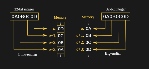
举例说明 Verilog 中的 Endianness:
module inv(input logic [3:0] a,
           output logic [3:0] y);

  assign y = ~a;
endmodule
2
3
4
5
a [3:0] 用来表示 4bits 的 bus (bunch of singnal),这里使用的是小端法。 因为 a [3] 可以理解为内存的最高位置,a [0] 理解为内存的最低位置,如果存在一个四个 bit 的数 1100 ,那么最高位 (1) 按照从左到右的顺序存放到 a [3],最低位 (0) 存放到 a [0] 中,按照 endianness 的规则,二进制数的最低位存放到了内存的最低位置,所以是小端法。
同理,a [0:3] 用来表示大端法。
# Logic Gates
module gates(input logic  [3:0] a, b,
             output logic [3:0] y1, y2,
                                y3, y4, y5)

/* five different two-input logic
   gates acting on 4-bit busses
   下面的语句都是并行运行,并不是顺序运行 */
  assign y1 = a & b;    // AND
  assign y2 = a | b;    // OR
  assign y3 = a ^ b;    // XOR
  assign y4 = ~(a & b);    // NAND
  assign y5 = ~(a | b);    // NOR
2
3
4
5
6
7
8
9
10
11
12
Operator:
&, |, ...Operand:
a, b,...Expression:
a & bStatement:
assign y1 = a & b;,Continuous assignment statements:
assign out = in1 op in2;
(Continuous assignment statements: 赋值符号左边的输入发生改变,赋值符号右边的输入需要立刻进行重新计算。 这符合组合逻辑电路的特点,所以使用 Continuous assignment statements 来描述组合逻辑,并且assign标识的语句都是并行运行的。)
# 4.2.2 Conditional Assignment
Verilog 中注释的写法和 C 语言中一摸一样,可以使用 /**/ 或者 // 。
# 4.2.3 Reduction Operators
(规约运算符, 目的为了书写简单)
OR, XOR, NAND, NOR, XNOR 都有规约运算符:
| Operator | Reduce Type |
|---|---|
| & | And |
| ~& | Nand |
| | | Or |
| ~| | Nor |
| ^ | XOR |
| ~^ | XNOR |
module and8(input  logic[7:0] a,
            output logic      y);
  assign y=&a;

  // &a is much easier to write than
  // assign y = a[7] & a[6] & a[5] & a[4] &
  // a[3] & a[2] & a[1] & a[0];
endmodule
2
3
4
5
6
7
8
# 4.2.4 Conditional Assignment
(也叫做三元运算符 ?: ,和 C 语言中的使用方法一样)
使用 Conditional Assignment 实现 4:1 的 MUX:
module mux4(input logic [3:0] d0, d1, d2, d3,
            input logic [1:0] s,
            output logic [3:0] y);
  assign y = s[1] ? (s[0] ? d3 : d2)
                  : (s[0] ? d1 : d0);
endmodule
2
3
4
5
6
当 s[1] = 1 时:
s[0] = 1,s = 11,此时y = d3s[0] = 0,s = 10,此时y = d2
当s[1] = 0时:s[0] = 1,s = 01,此时y = d1s[0] = 0,s = 00,此时y = d0
即一个 4:1 MUX。
# 4.2.5 Internal Variables
将复杂的函数功能分为多个步骤实现,其中中间步骤使用中间变量 (Internal variables) 表示:
Input -> 中间步骤 -> 中间步骤 -> 输出
举例 2.8.3 Full Adder:
根据全加器的真值表画出卡诺图,可以得到全加器的输出 S 和进位输出
所以可以令
其中 P 和 G 均称为中间变量 (类似于 C 语言函数中的局部变量)。
HDL 语言描述全加器:
module fulladder(input logic  a, b, cin
                 output logic s, cout);
/* In verilog, internal signals are
   usually declared as `logic`*/
   logic p, g;

   assign p = a ^ b;
   assign g = a & b;

   assign s = p ^ cin;
   assign cout = g | (p & cin)
endmodule
2
3
4
5
6
7
8
9
10
11
12
# 4.2.6 Precedence
SystemVerilog 中的操作符优先级:
| ~ | NOT |
|---|---|
| *, /, % | MUL, DIV, MOD |
| +, – | PLUS, MINUS |
| <<, >> | Logical Left/Right Shift |
| <<<, >>> | Arithmetic Left/Right Shift |
| <, <=, >, >= | Relative Comparison |
| ==, != | Equality Comparison |
| &, ~& | AND, NAND |
| ^, ~^ | XOR, XNOR |
| |, ~| | OR, NOR |
| ?: | Conditional |
# 4.2.7 Numbers
数字在 SystemVerilog 中可以指定为二进制,八进制,十进制和十六进制的形式。
语法格式:
N'Bvalue
- N 表示有多少个 bit
如果没有指定,那么 N 和存储数字的变量有相同的大小 (比如 w 为 6bit,则assign w = 'b11'会将000011赋值给 w)。 - B 表示进制 (
'bfor binary,'ofor octal,'dfor decimal,'hfor hexadecimal)。 '0和'1分别表示将全 0 和全 1 赋值给变量。- 下划线
_在 value 中只是为了帮助断句,增加可读性。 - 一个没有给定 N 和进制的数,默认为 10 进制。
举例:
| Numbers | Bits | Base | Val(Decimal) | Stored |
|---|---|---|---|---|
| 3'b101 | 3 | 2 | 5 | 101 |
| 'b11 | ?(取决于变量) | 2 | 3 | 00...0011 |
| 8'b11 | 8 | 2 | 3 | 00000011 |
| 8'b1010_1011 | 8 | 2 | 171 | 10101011 |
| 42 | ?(取决于变量) | 10 | 42 | 00..0101010 |
# 4.2.8 Z's and X's
同 2.6 X's and Z's,在 HDL 用 z 来表示浮动值 (floating value); 用 x 来表示无效的逻辑电平 (invalid logic level)。
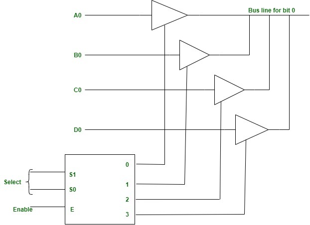
- 当三态缓存 (Tristate Buffer) enable 端为 0 时,输出为浮动值,所以三态缓存的 HDL 描述为:
module trisate(input logic [3:0] a,
               input logic      en,
               output tri  [3:0] y);

  assign y = en ? a : 4'bz
endmodule
2
3
4
5
6
警告
tri 是什么?nets 是什么?
- 在开始 HDL 仿真时,触发器的输出端都会被设定为
x用来表示未知的状态。
在 SystemVerilog 中输入可能有四种情况:
| Value | Definition |
|---|---|
| 0 | Logic zero or false |
| 1 | Logic one or true |
| x | Unknown logical value |
| z | Float value |
- 对于以上输入,AND 的真值表为:

# 4.2.9 Bit Swizzling
使用复制算子和拼接算子将变量和常量可以混合组成信号。
# 复制算子与拼接算子
- 复制算子: {num {vector}}
- 拼接算: {a,b,c} 子
举例:
assign y = {c[2:1], {3{d[0]}}, c[0], 3'b101};
其中 bracket {} 在 verilog 中表示为连接操作符 (concatenate operator), 连接操作符的操作数可以是多种数据类型。
assign y = {c[2:1], c[0], 3'b101};
另外 bracket {} 还可以作为 Replication Operator,用来重复一组 bits:
assign y = {3{d[0]}};
# 4.2.10 Delays
在 Verilog 中还可以在任意位置加入 delay,举例如下:
timescale 1ns/1ps

module example(input  logic a, b, c,
               output logic y);

  logic ab, bb, cb, n1, n2, n3;  # interval vriables

  assign #1 {ab, bb, cb} = ~{a, b, c}; # Inverters have a delay of 1ns
  assign #2 n1=ab & bb & cb;  # AND gates have a dealy of 2ns
  assign #2 n2=a & bb & cb;
  assign #2 n3 = a & bb & c;
  assign #4 y=n1 | n2 | n3;   # OR gates have a delay of 4ns
endmodule
2
3
4
5
6
7
8
9
10
11
12
13
timescale unit/precision用来指定单位时间的大小,本例中表示单位时间为 1ns,仿真精度为 1ps。如果没有指定,默认通常为单位时间为 1ns,仿真精度为 1ns。#用来表示延迟的数量,可以被放置在assign,<=,=关键字后 (后两个关键字在 4.5.4 中进行介绍)。
# 4.3 Structural Modeling
4.2 节主要是 behavioral Modeling,描述一个模块的输入输出的关系;
本节将主要描述使用简单的模块构建复杂的模块,即结构模型 (structural modeling)
下面的例子展示了如何使用 3 个 2:1 的 MUX 组成 4:1 的 MUX,MUX 在 2.8.1 节介绍。
其中 lowmux, highmux, finalmux 都是 mux2 的实例 (instance),这也是我们在第一章中所介绍的管理复杂度的一个原则 regularity
module mux4(input logic [3:0] d0, d1, d2, d3,
            input logic [1:0] s,
            output logic [3:0] y);
  logic [3:0] low, high;
  mux2 lowmux(d0, d1, s[0], low);
  mux2 highmux(d2, d3, s[0], high);
  mux2 finalmux(low, high, s[1], y);
endmodule
2
3
4
5
6
7
8
9
mux2 模块的定义见 4.5, 4.15, 4,34.
使用三态缓存构建 MUX2 的 verilog 实现为 (不推荐使用三态缓存构建 MUX):
module mux2(input logic[3:0]d0, d1,
            input logic s,
            output tri [3:0]y);
  trisate(d0, ~s, y);
  trisate(d1, s, y);
2
3
4
5
使用两个 4bit 宽度的 2:1MUX 组成一个 8bit 宽度的 2:1MUX:
module mux2_8(input logic [7:0]d0, d1,
              input logic [7:0] s,
              output logic [7:0] y);
  mux2 lsbmux(d0[3:0], d1[3:0], s, y[3:0]);
  mux2 lsbmux(d0[7:4], d1[7:4], s, y[7:4]);
2
3
4
5
这充分的体现了层次体系 hierarchy 的设计,在高的层次,我们更加关注结构的设计,即如何将不同的模块连接起来组成高层级的电路 (比如这里的 8bit 的 2:1MUX),而在较低的层次,我们更加注意行为设计 (比如一个 2:1MUX 应该由哪些门电路组成)。
# 4.4 Sequential Logic
# 4.4.1 Registers
always : 如果 always 语句的 sensitivity list (敏感列表) 中的事件发生, always 语句监控的语句会执行,否则信号会保持原始值。
因此可以使用 always 语句来表示带有记忆的电路。(时序逻辑电路)
对应的, assign 语句用来描述组合逻辑电路,只要语句等号右变的信号发生改变,左边就会立即发生响应。
always 语句的格式:
always @(sensitivity list)
  statement;
2
statement只有在senditivity list发生时才会执行sensitivity list(敏感列表) 也被称为stimulus list<=被称为nonblocking assignment(非阻塞赋值),具体介绍看 Section 4.5.4- 使用
always语句可以写出触发器,锁存器和组合电路,所以引入了:always_ff表示触发器always_latch表示锁存器always_comb表示组合电路
(通过这种方法,如果你的always_xx语句中综合出的逻辑电路不是 xx 功能的话,verilog 工具就会报错;比如在always_ff语句中实现了一个组合逻辑,就会报错)
笔记
在 verilog 中没有 always_comb ,所以使用 always@(*) 代替 always_comb ,其他情况都使用 always 。
- 下面的例子中
q<=d读作 "q gets d"
(这个 @符号,让我想起了 python 中的 wrapper)
D 触发器的 verilog 描述如下:
module flop(input logic clk,
            input logic [3:0] d,
            output logic [3:0] q);

  always_ff @(posedge clk)
    q<= d;
endmodule
2
3
4
5
6
7
# 4.4.2 Resettable Registers
关于可复位触发器在 3.2.6 已经进行过具体的讲解,这里只给出 verilog 表示
Synchronously resettable flip-flops (同步可复位触发器) 的 verilog 描述:
module flopr(input logic clk,
             input logic reset,
             input logic [3:0] d,
             output logic [3:0] q);
  // synchronous reset
  always_ff @(posedge clk)
    if (reset) q <= 4'b0;
    else q <= d;
endmodule
2
3
4
5
6
7
8
9
Asynchronously resettable flip-flops (异步可复位触发器):
module flopr(input logic clk,
             input logic reset,
             input logic [3:0] d,
             output logic [3:0] q);
  // asynchronous reset
  always_ff @(posedge clk, posedge reset) // always_ff @(posedge clk or posedge reset)
  if (reset) q <= 4'b0;
  else q <= d;
endmodule
2
3
4
5
6
7
8
9
注意
在 sensitivity list (敏感列表) 中如果有多个信号,则使用 comma 或者 or 进行分隔。
笔记
在 verilog synthesize (综合) 产生的 schematic (图解) 中难以区分异步和同步可复位触发器,比如在 Synplify Premier 产生的结果中,异步的复位信号在触发器的下方,同步电路的复位信号在触发器的左方。
# 4.4.3 Enabled Registers
电平启动的触发器的具体描述见 3.2.5
电平启动的异步可复位触发器的 verilog 描述如下:
module flopenr(input logic clk,
               input logic reset,
               input logic en,
               input logic [3:0] d,
               output logic [3:0] q);
  // asynchronous reset
  always_ff @(posedge clk, posedge reset)
    if (reset) q <= 4'b0;
    else if (en) q <= d; endmodule
2
3
4
5
6
7
8
9
(在上升沿时,只有当 reset 和 en 都为 FALSE 时触发器的信号才保持原值。)
# 4.4.4 Multiple Registers
在一个 always 语句中也可以描述多个硬件,比如将两个触发器串联:
module sync(input logic clk,
            input logic d,
            output logic q);
  logic n1;
  always_ff @(posedge clk)
    begin
      n1 <= d; // nonblocking
      q<= n1; // nonblocking
    end
endmodule
2
3
4
5
6
7
8
9
10
笔记
begin/end 结构类似与 C 语言中的 block {} 中的语句。
# 4.4.5 Latches
D 锁存器的 verilog 描述如下:
module latch(input logic clk,
             input logic [3:0] d,
             output logic [3:0] q);
  always_latch // 等价于 always@(clk, d)
    if (clk) q <= d;
endmodule
2
3
4
5
6
注意
并不是所有的 synthesis tool (综合工具) 都支持 D 锁存器。
# 4.5 More Combinational logic
在上面的例子中,我们都是使用 assign 描述组合逻辑电路,使用 always 描述时序逻辑电路。
使用 always 实现 inverter 的 verilog 描述:
module inv(input logic [3:0] a,
           output logic [3:0] y);
  always_comb // 等价于always @(a)
    y = ~a;
endmodule
2
3
4
5
不使用 always 语句的 inverter 描述见 4.2
使用 always 实现 full adder 的 verilog 描述:
module fulladder(input logic a, b, cin,
                 output logic s, cout
  );
  logic p, g;

  always_comb // 等价于always @(a, b, cin)
    begin
      p = a ^ b; // blocking
      g = a & b; // blocking
      s = p ^ cin; // blocking
      cout = g | (p & cin); // blocking end endmodule
    end
endmodule
2
3
4
5
6
7
8
9
10
11
12
13
不使用 always 语句的 full addere 描述见 4.2.5
使用 always 描述组合逻辑电路时:
always_comb等价于always @(*),但是最好使用always_comb因为如果在always_comb中描述的不是组合逻辑电路就会报错。- 在上面 inverter 的例子中,
always_comb还等价于alway @(a) - 如果 verilog 的
always语句满足下列两个条件,那么always语句一定描述了组合逻辑电路,always语句就可以替换会always_comb。always对所有的输入都会发生响应always的 body 语句中描述了所有的输入组合情况
(D 锁存器就是缺乏了第二个条件。)
- 使用 blocking assignment (
=) 来描述组合逻辑- 一组 blocking assignment 是串行来进行 evaluation 的
- 使用 nonblocking assignment (
<=) 来描述时序组合逻辑- 一组 nonblocking assignment 是并行来进行 evaluation 的
(为什么见 4.5.4 节)
- 一组 nonblocking assignment 是并行来进行 evaluation 的
笔记
nonblocking assignment 和 blocking assignment 都是用在 always 的 body 中。
assign 用在 always 语句外面,并且是并行评估的。
always @(*)什么时候被evaluation?
我从 NJU 的 DDCA 实验 (opens new window)中了解到,* 号将自动包含 always 语句块中语句右边或条件表达式出现的所有信号,示例请看链接。
# Case Statements
注意
case只允许在 always 语句中使用。- 使用
case实现组合逻辑时,必须有 default,以防出现锁存器 (也可以在 case 前给所有的输出赋值,从而不需要使用 default,举例见 USTC OJ - 避免锁存器 (opens new window)),或者见 NJU DDCA 实验 (opens new window) - case 语句中每个条目只执行一条语句,如要在一个条目下进行多个赋值,需要将多条预计放在 begin/end 关键字之间
使用真值表 + 卡诺图的方法设计七段数码管的设计是容易出错的,因为要为每个段写一个逻辑表达式。verilog 提供了 case 语句 (多路分支语句) 来实现七段数码管:
module sevenseg(input logic [3:0] data,
                output logic [6:0] segments
);
always_comb
  case(data)
    //               abc_defg
    0: segments = 7'b111_1110;
    1: segments = 7'b011_0000;
    2: segments = 7'b110_1101;
    3: segments = 7'b111_1001;
    4: segments = 7'b011_0011;
    5: segments = 7'b101_1011;
    6: segments = 7'b101_1111;
    7: segments = 7'b111_0000;
    8: segments = 7'b111_1111;
    9: segments = 7'b111_0011;
    default: segments = 7'b000_0000;
  endcase
endmodule
2
3
4
5
6
7
8
9
10
11
12
13
14
15
16
17
18
19
(书上 7.2.2 节七段数码管的 verilog 实现。)
使用 case 实现 3:8 的 decoder:
module decoder3_8(input logic [2:0] a,
                  output logic [7:0] y
);
always_comb
  case(a)
    3'b000: y = 8'b00000001;
    3'b001: y = 8'b00000010;
    3'b010: y = 8'b00000100;
    3'b011: y = 8'b00001000;
    3'b100: y = 8'b00010000;
    3'b101: y = 8'b00100000;
    3'b110: y = 8'b01000000;
    3'b111: y = 8'b10000000;
    default: y = 8'bxxxxxxxx; // (仿真时输入可能为x或者z,此时执行default)
  endcase
endmodule
2
3
4
5
6
7
8
9
10
11
12
13
14
15
16
使用 casez 中支持 don't care,
举例 Priority Circuit using don't care:
module priority_casez(input logic [3:0] a,
                      output logic [3:0] y
);

  always_comb casez(a)
    4'b1???: y = 4'b1000;
    4'b01??: y = 4'b0100;
    4'b001?: y = 4'b0010;
    4'b0001: y = 4'b0001;
    default: y = 4'b0000;
endcase endmodule
2
3
4
5
6
7
8
9
10
11
# 4.5.2 If Statements
注意
if 只允许在 always 语句中使用。
2.4 节优先级电路的 verilog 表述为:
module priorityckt(input logic [3:0] a,
                   output logic [3:0] y
);

  always_comb // 等价于always@(*)
    if (a[3]) y <= 4'b1000;
    else if (a[2]) y <= 4'b0100;
    else if (a[1]) y <= 4'b0010;
    else if (a[0]) y <= 4'b0001;
    else y <= 4'b0000;
endmodule
2
3
4
5
6
7
8
9
10
11
和 section4.5 always 中的处理一样:
- 如果 verilog 的
always语句满足下列两个条件,那么always语句一定描述了组合逻辑电路。
(always语句就可以替换会always_comb,只在 system verilog 中有效,verilog 中没有always_comb)。always对所有的输入都会发生响应always的 body 语句中描述了所有的输入组合情况
注意
语法正确的代码并不一定能产生功能正常的电路,一般来说都是因为不小心引入了锁存器造成的。举例 if 不完备产生锁存器 (opens new window)
if不完备可能导致的另一个问题
编译器判断 if 后面的条件表达式是否满足,如果满足则执行其后的语句,那如果条件表达式不满足呢?这时,编译器就会自动产生一个寄存器来寄存当前的值,在条件不满足时保输出的过去值。这样就会产生用户没有设计的多余的寄存器出来。
资料:NJU DDCA 实验 (opens new window)
# 4.5.3 Truth Tables with Don't Cares
在 Verilog 中使用 ? 描述真值表中的 don't cares:
因此,优先级电路也可以用如下的方式表示:
module priority_casez(input logic [3:0] a,
                      output logic [3:0] y
);

always_comb
  casez(a)
    4'b1???: y <= 4'b1000;
    4'b01??: y <= 4'b0100;
    4'b001?: y <= 4'b0010;
    4'b0001: y <= 4'b0001;
    default: y <= 4'b0000;
  endcase
endmodule
2
3
4
5
6
7
8
9
10
11
12
13
警告
为什么这里要使用 <= ,不是说组合逻辑都使用 = ?
笔记
casez 可以识别 ? 为 don't cares,除此之外,其他行为和 case 一致。
# 4.5.4 Blocking and Nonblocking Assignments
(本节非常重要)
在 always 语句中 = : Blocking Assignment
在 always 语句中 <= : Nonblocking Assignment
- 对于同步时序逻辑电路使用 always@(posedge clk) 和 nonblocking assignment (非阻塞赋值 (a <= b),并行)
- 对于简单的组合逻辑电路使用 continuous assignment (连续赋值
assign) - 对于较为复杂的组合逻辑电路使用
always@(*)和 blocking assignment (阻塞赋值 (a = b),串行) - 不要在多个 always 语句或连续赋值
assign语句中给同一个信号赋值,这样做可能会导致信号值不确定。
组合逻辑电路的 always 块与 assign 语句等效,用户描述组合逻辑电路时,可根据便利性选择其中一种方式使用。两者生成的硬件电路一般是等效的,但在语法规则上稍有不同:
-assign 语句只能对一个信号进行赋值,always 块内可对多个信号进行赋值
- assign 语句中被赋值信号为 wire 类型,always 块内被赋值信号需定义为 reg 类型,这仅仅是语法上面的要求,具体参考 4.7 Data Types
-always 块内支持更加丰富的语法,如使用 if…else..、case 等适合实现交复杂的组合逻辑
为什么不要在组合逻辑中使用非阻塞赋值?
- 在全加器的例子中使用 blocking assignment:
假设 a = 0, b = 0, cin = 0, 因此 p = 0, g = 0, s = 0;
- 因为是阻塞赋值,当 a: 0 -> 1, 此时
always中的语句会串行执行:输入:a = 1, b = 0, cin = 0 1. p: 1 ^ 0 = 1 2. g: 1 & 0 = 0 3. s: 1 ^ 0 = 1 4. cout: 0 | (1 & 0) = 01
2
3
4
5
- 如果在全加器的例子中使用 nonblocking assignment:
/ nonblocking assignments (not recommended)
module fulladder(input logic a, b, cin,
                 output logic s, cout
);

  logic p, g;

  always_comb
    begin
      p<= a ^ b; // nonblocking
      g<= a & b; // nonblocking
      s<= p ^ cin;
      cout <= g | (p & cin);
    end
endmodule
2
3
4
5
6
7
8
9
10
11
12
13
14
15
- 因为是非阻塞赋值,当 a: 0 -> 1, 此时
always中的语句会并行执行:初始状态: a = 0, b = 0, cin = 0, p = 0, g = 0, s = 0, cout = 0 | | a(0 -> 1导致`always`语句被执行): a = 1, b = 0, cin = 0 | a改变导致: p = 1 ^ 0 = 1, g = 1 & 0 = 0, s = 0 ^ 0 = 0, cout = 0 | (0 & 0) = 0(因为p和s是并行计算,所以s用的是p的old value) | | p(0 -> 1导致`always`语句再次被执行): a = 1, b = 0, cin = 0 | p改变导致: p = 1 ^ 0 = 1, g = 1 & 0 = 0, s = 1 ^ 0 = 1, cout = 0 | (1 & 0) = 01
2
3
4
5
6
7
8
9
笔记
虽然在这里得 full adder 使用 nonblocking assignment 最终达到的结果和使用 blocking assignmet 达到的结果是相同的,但是前者的
always语句 evaluation 了两次,但是后者的always语句只 evaluation 了一次,说明在组合逻辑中使用前者会使得仿真变慢。如果使用 always@(*),
always语句外面的中间变量发生变化也会导致always语句被执行,但是如果使用的是 always@(input...), 那么如果忘记将always语句外面的中间变量加入 sensitive list 中,那么当中间变量发生变化时,不会导致always语句再次被执行而产生错误。(比如上面例子中的如果写为always@(a, b, cin)那么 alwasy 只会执行一次,最后 s 只会为 0)一些 synthesis tool (综合工具) 在错误的 sensitive list 中可能产生正确的硬件,但是仿真时可能会发生错误,导致仿真结果和实际硬件的结果不一致。
为什么不要在同步时序逻辑电路中使用阻塞赋值?
对于 synchronizer 的例子,如果使用非阻塞赋值:
module sync(input logic clk,
            input logic d,
            output logic q);
  logic n1;
  always_ff @(posedge clk)
    begin
      n1 <= d; // nonblocking
      q<= n1; // nonblocking
    end
endmodule
2
3
4
5
6
7
8
9
10
- 因为是非阻塞赋值,假设 d = 0, n1 = 1, q = 0,当上升沿到来时,
always中的语句并行执行:n1 = 0 q = 11
2
对于 synchronizer 的例子,如果使用阻塞赋值:
module sync(input logic clk,
            input logic d,
            output logic q);
  logic n1;
  always_ff @(posedge clk)
    begin
      n1 = d; // blocking
      q = n1; // blocking
    end
endmodule
2
3
4
5
6
7
8
9
10
- 因为是非阻塞赋值,假设 d = 0, n1 = 1, q = 0,当上升沿到来时,
always中的语句串行执行:n1 = 0 q = 01
2
因为 n1 是中间变量,可能会被 synthesizer 优化掉,从而导致错误。
# 4.6 Finite State Machine
看懂 Section 3.4.3 就能理解
# 4.7 Data Types
Verilog 中有两种数据类型: wire 和 reg
reg不一定是寄存器,触发器,锁存器的输出,也可以是组合逻辑电路的输出- 在
always语句中<=(nonblock) 和=(block) assignment 的 LHS 必须使用reg类型 input和output在没有显示声明为reg类型的情况下,默认为wire类型 (在下面的例子中 clk 和 d 为 wire 类型,q 为 reg 类型)
module flop(input clk,
            input [3:0] d,
            output reg [3:0] q
);

always @(posedge clk)
  q<= d;

endmodule
2
3
4
5
6
7
8
9
对于 SystemVerilog 中还有其他的数据类型:
- logic: logic 是数据类型 reg 的同义替换,但是也有一点不同:
reg类型在 Verilog 中只能用在always中,在 SystemVerilog 中 logic 类型还可以用在assign语句中 - tri 和 wire 属于同义的数据类型,但是一个 wire 只能有一个驱动器,但是 tri 可以有多个驱动器。
比如下图中的总线就有四个驱动器,所以要将总线,即三态门的输出声明为tri类型。
- 在 SystemVerilog 中的数都默认为无符号类型,使用
signedmodifer (修饰符) 表示有符号数。
// 4.33(a): unsigned multiplier
module multiplier(input logic [3:0] a, b,
                  output logic [7:0] y
);
  assign y = a*b;
endmodule

// 4.33(b): signed multiplier
module multiplier(input logic signed [3:0] a, b,
                  output logic signed [7:0] y
);
  assign y = a * b
endmodule
2
3
4
5
6
7
8
9
10
11
12
13
# 4.6 Finite State Machine
有限状态机在课本的 Section 3.4 (opens new window) 章节。
verilog 是一种 HDL (Hardware Description Language),所以应该是根据 Section 3.4 有了 FSM 的状态转化图后,再去写 verilog
书上给了 divideby3 的 Moore 实现对应的 system verilog 描述;sail pattern 的 Moore 和 Mealy 实现对应的 system verilog 描述。
其中 divideby3 是书上 Section 3.4.2 节的例子 (P130 页),system verilog 语言描述为:
module divideby3FSM(input logic clk,
                    input logic reset,
                    output logic y
);
  typedef enum logic [1:0] {S0, S1, S2} statetype; //如果未指定编码方式,使用binary encoding,即S0 = 00, S1 = 01, S2 = 10
  statetype [1:0] state, nextstate;

  // state register
  always_ff @(posedge clk, posedge reset)
    if (reset) state <= S0;
    else state <= nextstate;

  // next state logic
  always_comb
    case (state) S0: nextstate <= S1;
      S1: nextstate <= S2;
      S2: nextstate <= S0;
      default: nextstate <= S0;
    endcase

  // output logic
  assign y = (state == S0); endmodule
2
3
4
5
6
7
8
9
10
11
12
13
14
15
16
17
18
19
20
21
22
因为 Verilog 中没有关键字 typedef , enum , logic , always_ff ,上面的 system veirlog 对应的 verilog 为:
module divideby3FSM(input clk,
                    input reset,
                    output y
);
  parameter s0 = 2'b00;
  parameter s1 = 2'b01;
  parameter s2 = 2'b10;

  // always中赋值符号右边的类型都要声明为reg(Secton 4.7)
  reg [1:0] state;
  reg [1:0] nextstate;

  // state register
  always @(posedge clk, posedge reset)
    if (reset) state <= S0;
    else state <= nextstate;

  // next state logic
  always @(*)
    case (state) S0: nextstate <= S1;
      S1: nextstate <= S2;
      S2: nextstate <= S0;
      default: nextstate <= S0;
    endcase

  // output logic
  assign y = (state == S0); endmodule
2
3
4
5
6
7
8
9
10
11
12
13
14
15
16
17
18
19
20
21
22
23
24
25
26
27
28
笔记
parameter 类似于 C 语言中的 Macro Definition
参考资料:Verilog 语法 - 有限状态机 (opens new window)
snail pattern 是课本上 Section 3.4.3 节中的例子,其 system verilog 的 mealy 描述为:
module patternMealy(input logic clk,
                    input logic reset,
                    input logic a,
                    output logic y
);
  typedef enum logic {S0, S1} statetype;
  statetype state, nextstate;

  // state register
  always_ff @(posedge clk, posedge reset)
    if (reset) state <= S0;
    else state <= nextstate;

  // next state logic
  always_comb
    case (state)
      S0: if (a) nextstate = S0;
          else nextstate = S1;
      S1: if (a) nextstate = S0;
          else nextstate = S1;
      default: nextstate = S0;
    endcase

    // output logic
    assign y = (a & state ==S1);

endmodule
2
3
4
5
6
7
8
9
10
11
12
13
14
15
16
17
18
19
20
21
22
23
24
25
26
27
对应的 snail pattern mealy 的 verilog 描述为:
module patternMealy(input logic clk,
                    input logic reset,
                    input logic a,
                    output logic y
);
  typedef enum logic {S0, S1} statetype;
  statetype state, nextstate;
  parameter S0 1'b0;
  parameter S1 1'b1;

  // state register
  always_ff @(posedge clk, posedge reset)
    if (reset) state <= S0;
    else state <= nextstate;

  // next state logic
  always_comb
    case (state)
      S0: if (a) nextstate = S0;
          else nextstate = S1;
      S1: if (a) nextstate = S0;
          else nextstate = S1;
      default: nextstate = S0;
    endcase

    // output logic
    assign y = (a & state ==S1);

endmodule
2
3
4
5
6
7
8
9
10
11
12
13
14
15
16
17
18
19
20
21
22
23
24
25
26
27
28
29
# 4.8 Parameterized Modules
目前为止,我们将的模块的输入和输出都是固定长度的,参数化模块使得模块可以有可变数量的变量。
举例:N-Bit 2:1 MUX
module mux2
  #(parameter width = 8)
  (input logic [width–1:0] d0, d1,
   input logic s,
   output logic [width–1:0] y
  );

  assign y = s ? d1 : d0;
endmodule
2
3
4
5
6
7
8
9
- #(pramameter . . .) 写在输入和输出定义前定义参数
- 上面的例子中表示参数 width 的宽度默认为 8bits
使用上面的 MUX 构成 8 位的 4:1 的 MUX:
module mux4_8(input logic [7:0] d0, d1, d2, d3,
              input logic [1:0] s,
              output logic [7:0] y
);
  logic [7:0] low, hi;

  mux2 lowmux(d0, d1, s[0], low);
  mux2 himux(d2, d3, s[0], hi);
  mux2 outmux(low, hi, s[1], y);
endmodule
2
3
4
5
6
7
8
9
10
使用上面的 2:1MUX 构成 12 位的 4:1MUX:
module mux4_12(input logic [11:0] d0, d1, d2, d3,
               input logic [1:0] s,
               output logic [11:0] y
);
  logic [11:0] low, hi;

  mux2 #(12) lowmux(d0, d1, s[0], low);
  mux2 #(12) himux(d2, d3, s[0], hi);
  mux2 #(12) outmux(low, hi, s[1], y);
endmodule
2
3
4
5
6
7
8
9
10
笔记
#(...) 表示定义和重载模块的参数,#... 表示时延。
module decoder
  #(parameter N = 3)
  (input logic [N–1:0] a,
   output logic [2**N–1:0] y
  );

  always_comb // Equal to always@(*)
    begin
      y = 0; // Blocking assignment
      y[a] = 1;
    end
endmodule
2
3
4
5
6
7
8
9
10
11
12
之前我们使用了 case (/pages/acc834/#case-statements) 实现 3:8 的 decoder,相比之下,使用参数模块的 decoder 实现更加简单。
在 verilog 和 system verilog 中,可以使用 generator 语句生成一定数量的硬件, generator 支持 for 和 if 语句,举例使用 for 级联产生 N 位相与的操作:
module andN
  #(parameter N = 8)
  (input logic [N–1:0] a,
   output logic y);

   genvar i;

  logic [N–1:0] x;

  generate
    assign x[0] = a[0];
    for(i=1; i<N; i=i+1) begin: forloop
      assign x[i] = a[i] & x[i–1];
     end
   endgenerate
  assign y = x[N–1];
endmodule
2
3
4
5
6
7
8
9
10
11
12
13
14
15
16
17
笔记
genvar声明一个非变量的索引- The begin in a generate for loop must be followed by a : and an arbitrary label (forloop, in this case).
# 4.9 Testbenches
testbench 是 verilog 中的一个模块,用来测试其他模块,被测试的模块被称为 device under test (DUT,有时也被称为 UUT, unit under test)。
testbench 模块输入信号到 DUT 中,然后检查 DUT 的输出是否正确,输入和理想的输出的组合被称作 test vectors。
比如我们可以对 4.4.1 节中的 sillyfunction 模块进行测试:
module testbench1();
  logic a, b, c, y;

  // instantiate device under test(DUT)
  sillyfunction dut(a, b, c, y);

  // apply inputs one at a time
  initial begin
    a = 0; b = 0; c = 0; #10;
    c = 1;               #10;
    b = 1; c = 0;        #10;
    c = 1;               #10;
    a = 1; b = 0; c = 0; #10;
    c = 1;               #10;
    b = 1; c = 0;        #10;
    c = 1;               #10;
  end
endmodule
2
3
4
5
6
7
8
9
10
11
12
13
14
15
16
17
18
笔记
initial语句只能在 testbanch 或者仿真时使用,不能进行合成实际的硬件,因为这里使用的是 blocking assignment,所以会顺序执行上面的语句。testbanch模块也可以用于仿真,但是不能合成硬件。- 设计者可以通过检查仿真结果的输出来判断 DUT 的实现是否正确。
带自动检测功能的 testbench :
module testbench2();
  logic a, b, c, y;

  // instantiate device under test
  sillyfunction dut(a, b, c, y);

  // apply inputs one at a time
  // checking results
  initial begin
    a = 0; b = 0; c = 0; #10;
    assert (y === 1) else $error("000 failed.");
    c = 1; #10;
    assert (y === 0) else $error("001 failed.");
    b = 1; c = 0; #10;
    assert (y === 0) else $error("010 failed.");
    c = 1; #10;
    assert (y === 0) else $error("011 failed.");
    a = 1; b = 0; c = 0; #10;
    assert (y === 1) else $error("100 failed.");
    c = 1; #10;
    assert (y === 1) else $error("101 failed.");
    b = 1; c = 0; #10;
    assert (y === 0) else $error("110 failed.");
    c = 1; #10;
    assert (y === 0) else $error("111 failed.");
  end
endmodule
2
3
4
5
6
7
8
9
10
11
12
13
14
15
16
17
18
19
20
21
22
23
24
25
26
27
笔记
- system verilog 中可以使用
assert ... else ...进行检测,但是在 verilog 中没有 assert。 - system verilog 中有
$error,但是 verilog 中没有,verilog 只能使用如下的形式进行检测。 - testbench 文件一般不包含任何输入输出信号
- 将被测模块实例化,被测模块的输入信号定义成 reg 类型,输出信号定义成 wire 类型。(verilog 中)
module testbench2();
  reg a, b, c;
  wire y;

  // instantiate device under test
  sillyfunction dut(a, b, c, y);

  // apply inputs one at a time
  // checking results
  initial begin
    a = 0; b = 0; c = 0; #10;
    if (y !== 1) $display("000 failed.");
    c = 1; #10;
    if (y !== 0) $display("001 failed.");
    b = 1; c = 0; #10;
    if (y !== 0) $display("010 failed.");
    c = 1; #10;
    if (y !== 0) $display("011 failed.");
    a = 1; b = 0; c = 0; #10;
    if (y !== 1) $display("100 failed.");
    c = 1; #10;
    if (y !== 1) $display("101 failed.");
    b = 1; c = 0; #10;
    if (y !== 0) $display("110 failed.");
    c = 1; #10;
    if (y !== 0) $display("111 failed.");
  end
endmodule
2
3
4
5
6
7
8
9
10
11
12
13
14
15
16
17
18
19
20
21
22
23
24
25
26
27
28
== 和 === 的区别:
What is the difference between == and === in Verilog? (opens new window)
在 system verilog 中还可以使用 test vector 文件进行正确性检测,详细介绍见课本。
# Module Instantiations
模块实例化有两种方法:
- connect-by-order (基于端口位置的实例化)
module mod_a ( input in1, input in2, output out );
  // Module body
  assign out = in1 & in2; //这只是一个简单的示例
endmodule

module top_module(input wa,input wb,output wc);
mod_a inst_name1(wa,wb,wc);
endmodule
2
3
4
5
6
7
8
- connect-by-name (基于端口名称的实例化)
module mod_a ( input in1, input in2, output out );
  // Module body
  assign out = in1 & in2; //这只是一个简单的示例
endmodule

module top_module(input wa,input wb,output wc);
mod_a 	inst_name2(
  .out(wc),
  .in1(wa),
  .in2(wb)
);
endmodule
2
3
4
5
6
7
8
9
10
11
12
笔记
- 推荐使用基于端口名称的例化方式,因为这种方式编写的代码可读性更强
- 模块调用就像是一个树形的层次结构,不允许循环调用,如 a 调用 b,b 又调用 a,也不允许模块调用自身,即在模块 c 中实例化模块 c
- 不允许在进程块(如 always、initial 等)或赋值语句(如 assign 语句)内进行模块实例化
- 模块的实例化名称可以自定义,如在同一模块中要对一个模块多次实例化,需要有不同的实例化名称
- 实例化名称可以与模块名称相同 (但是这样不利于阅读)
- 实例化模块时,需要注意端口信号的位宽相匹配
# 信号初始化
wire 信号的初始化:
wire [4:0] master_data_out = 5'b01100;
reg 信号初始化:
// reg declaration with initialization
reg [7:0] data_reg = 8'b10101011;

// Or
reg [7:0] data_reg;
initial data_reg = 8'b10101011;
2
3
4
5
6
initial 的使用方法:
initial
  [single statement]

// Or
initial begin
  [multiple statements]
end
2
3
4
5
6
7
注意
initial是不可综合的。initial只可以用来初始化reg,不能用来初始化wire
参考资料:
Are the initial conditions for reg and wires synthetizable in Verilog? (opens new window)